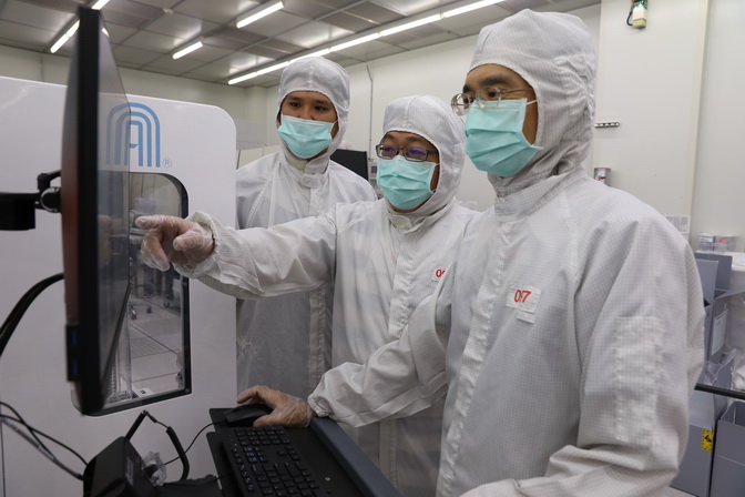
In response to the industrial and academic demands, resources inside and outside of TSRI are integrated to provide the semiconductor processing services of etching/thin film deposition, including atomic layer deposition and atomic layer etching for advanced material fabrication.
Services
Etching/thin film deposition services on coupon/6” /8” substrates.
Lithography Mask Service
Service description
In response to the industrial and academic demands, resources inside and outside of TSRI are integrated to provide the critical graphic design services in semiconductor processing. Services ranging from photo mask production, lithography process to the final stage of structural analysis are provided to facilitate research, development, and teaching needs of the industry and academia.
Services
4” /5” photo mask production service
Broken wafer; 6” /8” lithography process service
FIB/TEM sample preparation service
Process Integration Service
Service description
According to industrial dynamics and academic demand, the laboratory provides developers with a research and development service platform and resistive random-access memory service platform involving 3D device architecture sized 15 nm or smaller. Users can use the service platforms with other materials or change the manufacturing process to extend diversity in applications.
Services
Nonplanar device service platform
Resistive random-access memory service platform
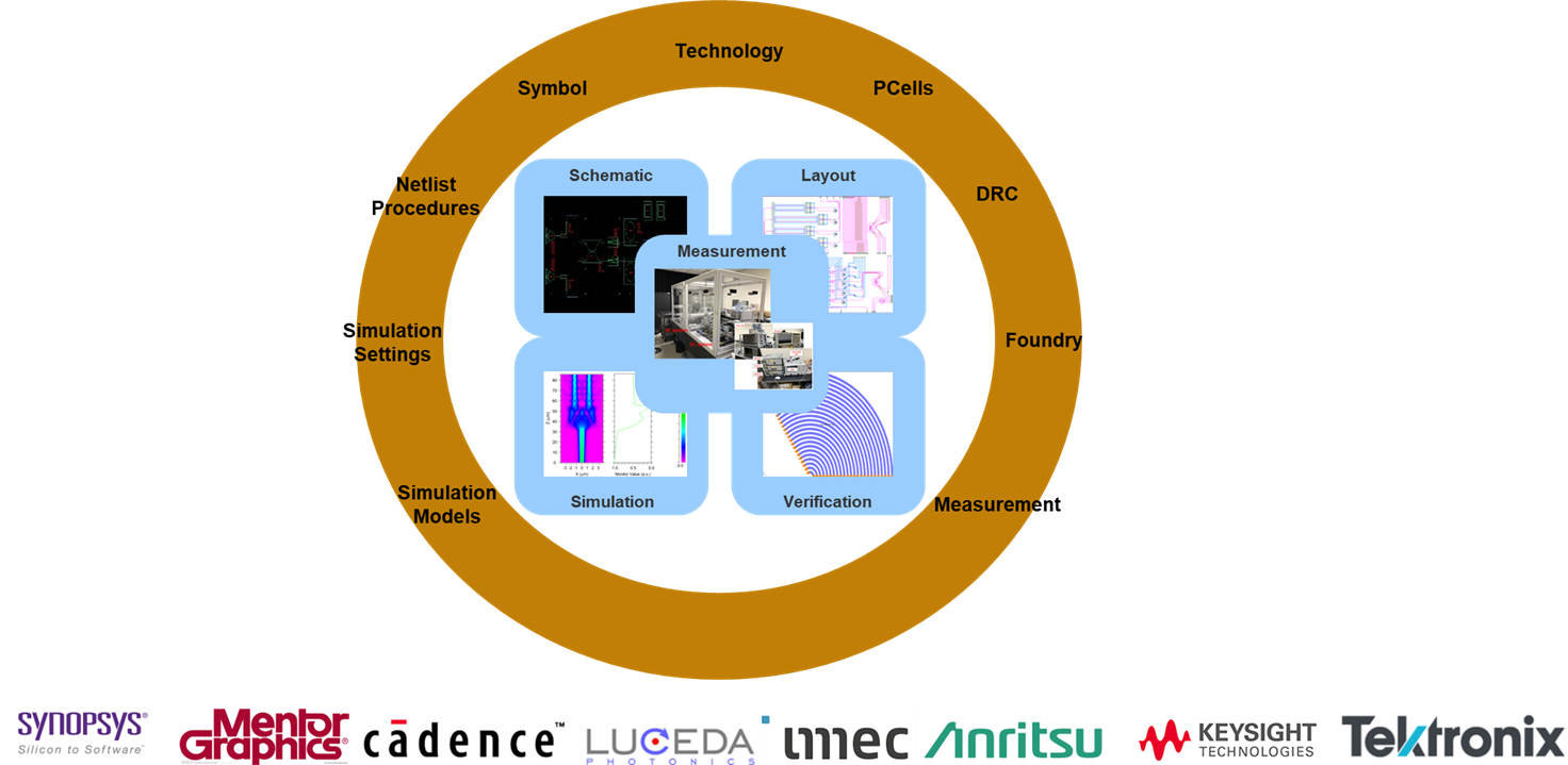
Silicon Photonic Technology and Service
Service description
Based on the silicon photonics international development trends and the needs of a Taiwanese academic team, TSRI integrates the EDA environment, wafer/chip fabrication environment and measurement equipment requirements environment, provides silicon photonics design, wafer/chip production, and measurement platforms to assist Taiwan academic teams in conducting silicon photonics research. At the same time, we cooperated with the academic team and international and Taiwan industry teams to develop key photonics technology.
Services
Provides software support for silicon photonics design, simulation, layout, and design rule checking
Assisting the academic team in chip/wafer fabrication of silicon photonics components and system designs
Silicon photonics measurement laboratory with component and system-level sample measurement services
Provides silicon photonics design and measurement training courses
Heterogeneous Integration Service
Service description
For the achievement of systematic heterogeneous device integration, sensor chip and system-in-2.5D/3D package are developed based on industrial development and heterogeneous academic demands, in order to provide a flexible package lab platform for Through-Silicon Via (TSV), chip thinning, and test chip bonding, etc. This is also offered for academic and industrial use and research.