Component Production

Device Technology

Smart Sensor Chip

Research description

Post-3nm technology node R&D platform.

Research focuses

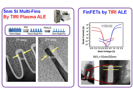
- Development of advanced semiconductor device structure technology.
  • FinFET.
  • Nanowire/Nanosheet transistor.
  • Stacked GAA transistor.
- Technology development for advanced semiconductor device channel and gate stack platform.
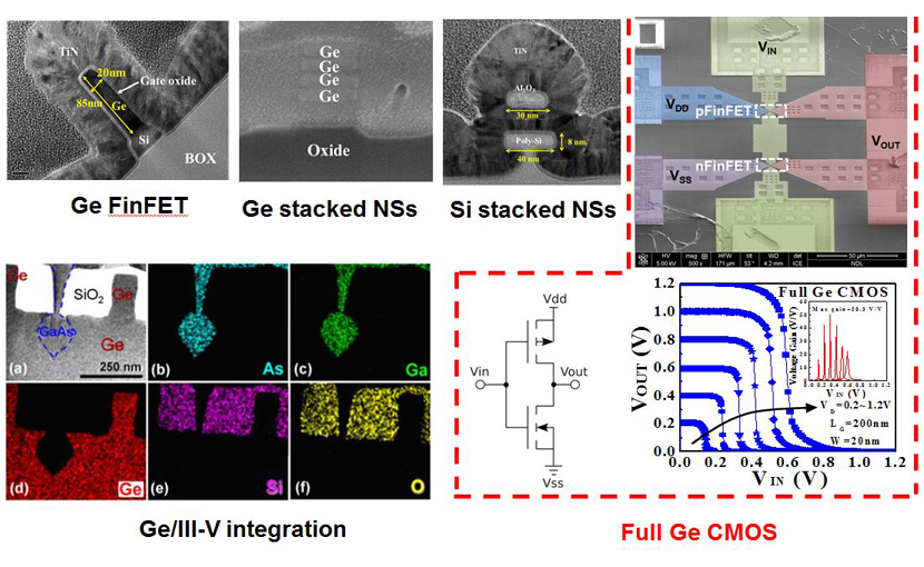
  • Group IV channel materials: Si, SiGe, Ge.
  • Group III-V channel materials: GaAs, InGaAs.
  • 2D channel materials.
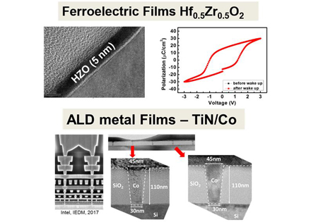
  • Ultrathin high-k gate dielectric and ferroelectric materials.

Research results

Develop 3D transistor technology suitable for post-3nm technology nodes and with high carrier mobility Ge channel and Group III-V channel.

Provide a R&D platform that is up to the industrial standard for domestic R&D teams to help with their research and development of advanced devices.

Atomic Layer Etching (ALE)

Smart Sensor Chip

Research description

ALE: Advanced etching process beyond 3-5nm-node semiconductor manufacturing technology, such as such as fabrication of quantum dots, nanowires, 2D materials, etc.

Research focuses

  • 3-5nm-node IC process.
  • Etching patterning of advanced memory materials.
  • Integration of GaN high-power devices.

Research results

Develop ALE processing technology suitable for technology nodes beyond 5nm.

Provide a flexible R&D laboratory environment that is up to the industrial standard for domestic R&D teams to help with their research and development of advanced components.

Atomic Layer Deposition (ALD)

Smart Sensor Chip

Research description

Research platform for ferroelectric thin film technology beyond 3-5nm.

Research focuses

Advanced HZO ferroelectric thin film technology.

Research results

Self-made ALD for HZO ferroelectric thin film deposition and transistor with subthreshold swing <<60mV/dec.

GaN Power Device Platform

GaN Power Device Platform

Research description

Next Generation GaN Green Power/RF Device.

Research focuses

  • Advanced GaN E-mode Power Device.
  • GaN RF Amplifier for 5G Communication.
  • High Frequency All-GaN IC.
  • High Thermal Conducting Power Device Package.

Research results

  • GaN 15A/650V E-mode Power Device.
  • Sub-6 GHz GaN RF Amplifier.
  • 2MHz All GaN Gate Driver.

Monolithic 3D+ IC Platform

Research description

Low thermal budget TSV-free FinFET-based 3D+ IC .

Research focuses

  • High data transmission speed.
  • High bandwidth.
  • Low power consumption and small footprint of integration Circuits.

Research results

Multi-functional circuits integration on single chip with small footprint and high data transmission speed.

Provide a flexible R&D laboratory environment that is up to the industrial standard for domestic R&D teams to help with their research and development of advanced circuits.